
Did you know that the global semiconductor silicon wafer market is projected to reach $13.64 billion by 2027?
Silicon wafers are crucial for producing electronic devices. From smartphones to computers, silicon wafers are the building blocks of modern technology.
Making silicon wafers involves intricate, precise steps that require expertise. In this document, we will explore the journey from sand to semiconductor. Keep reading to find out how are silicon wafers made!
Polysilicon Production
The first step in creating silicon wafers is producing polysilicon. Manufacturers do this by melting down raw silica sand. They then use a chemical process to purify the molten sand, removing any impurities.
The result is polysilicon, which has a purity level of over 99.9999%. This highly pure material is the foundation of silicon wafers.
This process is incredibly energy-intensive. It accounts for up to 80% of the total energy consumption in the wafer production.
Crystal Growth
The next step in making silicon wafers involves crystal growth. This process requires extreme precision and control to ensure a flawless final product.
To start, manufacturers put small pieces of polysilicon into a quartz crucible. They then heat the crucible to over 1500°C while simultaneously rotating it. As the crucible rotates, a silicon seed crystal is slowly lowered into the molten polysilicon.
As the crystallization process begins, the seed crystal acts as a template for the formation of a single large silicon crystal. This process can take up to several days to complete.
Here are the techniques used for crystal growth in the production of silicon wafers:
Czochralski Method
This is the most common technique used for crystal growth. It involves pulling the seed crystal out of the molten polysilicon at a controlled rate. This forms a cylindrical crystal.
The method is named after the Polish scientist who invented it in 1917, Jan Czochralski. It allows for the production of large, high-quality single crystals. This is suitable for making silicon wafers.
Float Zone Method
This method involves melting a small portion of a seed crystal and creating a molten zone. The seed crystal is then slowly pulled through the molten zone. This creates a single crystal.
The float zone method is more expensive and time-consuming than the Czochralski method. However, it results in even higher-purity crystals. This makes it ideal for producing wafers used in the production of semiconductors.
Bridgman Method
In this method, the seed crystal is slowly lowered into the molten polysilicon. They do this while being cooled from one end.
This creates a cylindrical crystal that can then be cut into wafers. This method is best suited for producing silicon wafers used in electronics like solar cells and transistors.
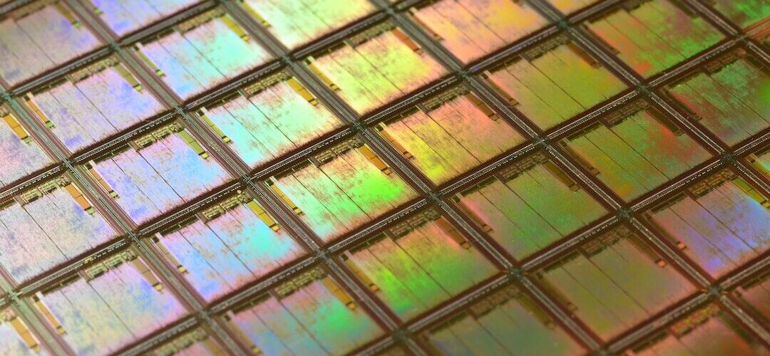
Wafer Slicing
After the crystals have been grown, they are then cut into thin slices known as wafers. This process involves using diamond saws or lasers to cut the cylindrical crystals.
Diamond Saws
Diamond saws cut the wafers from the cylindrical crystal. These saws are coated with diamond powder, which is the only substance harder than silicon.
The saws make precise cuts while minimizing material waste. However, they can result in rough edges and surface damage on the wafers.
Lasers
Some manufacturers use lasers instead of diamond saws for wafer slicing. This method is more precise and reduces material waste. It also results in smoother edges and surfaces on the wafers.
However, lasers are not as cost-effective as diamond saws and require more maintenance. This makes them less commonly used in wafer slicing.
Wafer Polishing
After the wafers have been cut, they go through a polishing process. This is to remove any imperfections and create a smooth surface. This is crucial for the successful production of electronic devices.
The wafers are placed in a rotating machine that uses chemical slurry and polishing pads. This process can take several hours until the wafers are smooth and shiny.
Etching
After wafer slicing, the wafers undergo a process called etching. This involves using chemicals to remove any impurities. This also smooths out the surface of the wafers.
Etching is crucial for ensuring that the wafers have a uniform thickness. This is important for the successful operation of electronic devices.
Moreover, patterns and circuits can also be etched onto the wafers during this process. This is known as photolithography. You can check silybwafers.com/ to learn more about wafer patterns.
Doping
Doping involves introducing impurities into the pure silicon material. These impurities create a specific electrical property in the wafers. This is necessary for the wafers to function as semiconductors.
Manufacturers use different types of doping agents. This depends on the desired electrical properties. Common dopants include boron and phosphorus.
Metallization
The metallization process involves depositing a thin layer of metal onto the wafer. This creates the electrical interconnections needed in the final device.
The most commonly used metal for this process is aluminum. This is due to its excellent conductivity and low cost.
Oxidation
This process involves exposing the wafers to high temperatures in an oxygen-rich environment. This creates a thin layer of silicon dioxide on the surface of the wafers.
This oxide layer serves as an insulator. It protects the underlying layers from damage. It also provides a surface for creating electronic components such as transistors.
Wafer Cleaning
The final step in producing silicon wafers is cleaning. The wafers undergo a cleaning process using chemicals and ultrasonic baths. This removes any remaining impurities.
This process also creates a smooth surface for the production of electronic devices. The cleaned wafers are then ready for use in the production of semiconductors.
Understanding How Are Silicon Wafers Made
Understanding how are silicon wafers made is crucial for electronic device production. The journey from sand to semiconductor involves several precise and meticulous steps. Each process plays a vital role in creating high-quality silicon wafers.
As technology advances, so will the techniques used in producing silicon wafers. The future of electronics relies on these tiny yet powerful building blocks. So, keep an eye out for future innovations in the production of silicon wafers!
Do you love reading informative content like this? If you do, then you’re in the right place. Keep browsing through our blog to find more content!


Add comment